
Leveraging our accumulated
technologies, equipment, and experience,
we aim to be a reliable partner for our customers.
Leveraging our accumulated
technologies, equipment,
and experience,
we aim to be a reliable
partner for our customers.
With know-how cultivated through the manufacturing of various semiconductor package types, we support a wide range of customer needs. Please feel free to contact us.



MANUFACTURING TECHNIQUE
We support the entrusted development with our know-how in many years. With our know-how which we have developed with semiconductor manufacturing experience of various package types, we appropriately meet the needs of customers. Please feel free to contact us.
Wafer Testing
We support electrical characteristic test (logic / LCD). We support low to high temperature tests.
Back Grinding / Dicing
Backside polishing
With a protection of wafer surface (front),
backside polishing polishes wafer backside to specified thickness.
We support for dividing wafer by backside polishing after wafer dicing.
* Available: ~ 300mm wafer
Laser grooving
Our laser grooving supports rigid board such as
Low-K materials which are difficult to be grooved
with blades.
* Available: ~ 300mm wafer
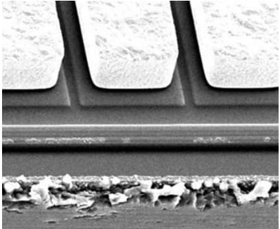
▲With laser grooving
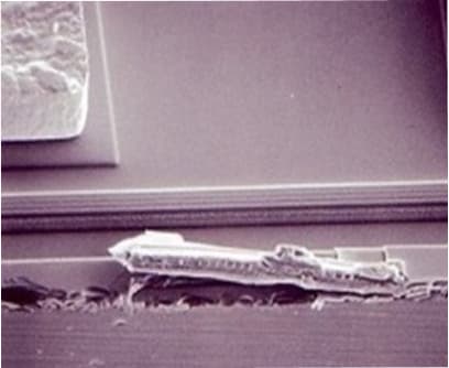
▲Without laser grooving
Dicing
Dicing is to make wafers, substrates, glasses, etc. into individual pieces.
With edge trimming, wafer cracking and chipping during backside polishing would be prevented.
*Available: ~ 300mm wafer
Back-end Assembly of LSI Devices
Die bonding
We support multi-layer / multiple die bonding.
We support various bonds (silver paste, plastic paste and film).
*Available: ~ 300mm wafer
Wire bonding
We support Au / Cn materials.
We support various wire bonding such as low loop, multi-layer and reverse.
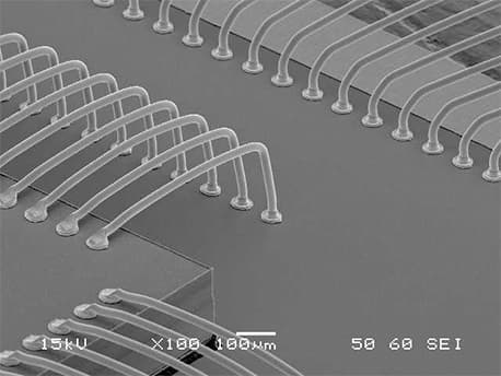
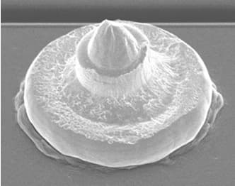
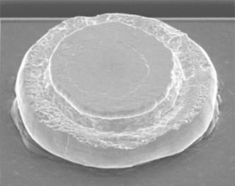
Bump bonding
We support low temperature Au bumping.
We support bare, tape mount and recon wafers.
*Available: ~ 300mm wafer
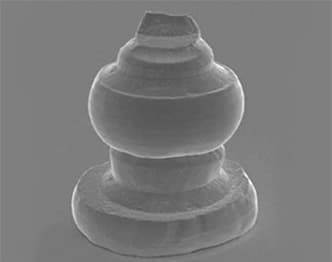
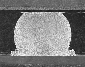
Flip chip bonding
We support chip mounting according to
requirements such as ceramic bards,
boards and FPC boards.
*Available: ~ 300mm wafer
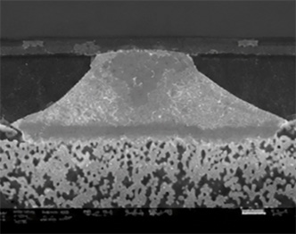
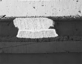
TCB(Thermal Compression Bonding)
We support high-density, fine-pitch assembly. By controlling the bonding height, we achieve stable interconnection quality.
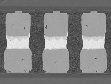
Molding
We select the molding according to the requirements such as transfer molding and compression molding.
Module Assembly
Surface mount technology (SMT)
We support the surface mount such as mounting micro chips. For a tiny area and high heat-dissipating area which are difficult to solder, we support with laser soldering machine. Also, we support the mounting of ultra-thin FPC on double-side. We select proper soldering from low-melting point to high-letting point according to the application.
Solder ball jet mounting
We support laser-based solder ball jet mounting. This method is suitable for fine-pitch components and enables reflow-less, flux-free assembly.
Fine wire batch soldering
We support batch soldering of ultra-fine wire cables. High-precision micro joining enables compatibility with AWG46 at a 0.2 mm pitch.
Final Test / Visual Inspection
Electrical test
We support electrical characteristic test (logic, LCD, module, imaging).
Appearance check
According to the needs of customers, we support appearance check with automatic inspecting machine and visual inspection.
Packaging / Delivery
Chip tray packaging
We support chip tray packaging with selecting good chips from the dicing completed wafer.
We support tray, tape and reel packaging.
ANALYSIS SERVICE
With our advanced analysing expertise and experience cultivated in the electronics industry, We provide full support from new product development to troubleshooting.
 Content Content |
|
|---|---|
| Electronic component diagnosis course | Analysis that can detect the presence or absence of defects. Observation of sample condition by utilizing the measuring microscope and optical microscope. Download Brochure |
| Analysis of foreign material contamination | Selection of the optimal analysis method and utilizing a precesion manipulator to collect particles with a few microns size. Observation + Particles Collection + Analysis + Report Download Brochure |
| Internal void, crack, and peeling analysis | Detection of inner voids, cracks and peeling defects in packages, metals, resins, etc. X-ray + SAT (ultrasonic inspection) + SEM observation Download Brochure |
| Cross-sectional sample preparation | Creating cross-sectional samples for analysis, observation and display. Observation + Cross-sectional polishing + Ion miling finishing Download Brochure |
| package opening | Advanced mold opening technique that does not damage the inside Laser opening + Chemical opening + Observation Download Brochure |
Equipment for Analysis
 Usage Usage |
Specification / Actual Cases |
|
|---|---|---|
| X-ray fluoroscopy machine | Seeing through the internal structure by irradiating the sample with X-rays. |
Focal spot size : 10μm Observation of ultrafine joint state of BGA/FBGA・P-PKG without destruction. |
| SEM-EDX | Identifying the constituent elements by observing the sample at high magnification with using X-rays. |
Sample observation: MAX x30,000 Composition analysis: Approx. 1μm Elemental analysis. |
| Tensile strength tester | Measuring the fracture strength by applying a certain force to the sample. |
Speed range: 0.001 - 1000mm/min (stepless setting) Sampling: Max. 1msec |
| SAT (Ultrasound Microscope) | Observing the internal damages by applying ultrasonic waves to the sample. |
Frequency: 30-100MHz Observation of physical defects inside the device without destruction. |
| 3D shape measuring machine | Converting the undulation and uneven shape of the sample into 3D data within a few seconds. | Comparison of stress before and after processing Flatness measurement |
| DSC | Identifying melting point and glass transition point from calorie change of the sample. |
Control range: -140℃~600℃ (when using liquid nitrogen) Calorie values can be calculated from the DSC peak of thermosetting resins such as mold resins to understand thermal characteristics and measure curing rate. |
| FT-IR | Identifying molecular structure of the sample from the amount of infrared absorption of organic substances. | Analysis of "organic foreign matter" less than 50μm. |
| Reflow simulator | Real time observation of behavior of the sample during reflow. |
Checking the melting temperature of the solder. Checking the curve of the board during heating. |
| Cross section polishing machine | Enabling the observation of cross section structure by cutting and polishing the sample. | Fine finishing without scratch, sagging or stretching according to the size, material and application of the sample. |
Reliability Test
We support reliability tests during product development with various environmental test equipment.
| Type | Operating Range & Application Range |
|---|---|
 Temperature cycle test Temperature cycle test |
High temperature: 60 to 200℃ Low temperature: -70 to 0 ℃ |
 Constant temperature and humidity test Constant temperature and humidity test |
Temperature: -20 to 100 ℃ Humidity: 20 to 98% RH |
 Pressure cooker test Pressure cooker test |
Temperature: 105 to 148.2 ℃ Humidity: 65 to 100% RH Pressure: 0 to 3atm |
 Low temperature test Low temperature test |
Temperature: -75 to 100℃ |
 Drop test Drop test |
Sample weight: up to 2 kg Sample dimensions: up to 150 mm Drop height: 200 to 2200mm |