


FLOW 01

Request
We support manufacturing products according to requirements of a customer.
Please feel free to contact us.
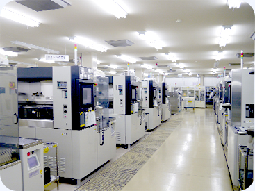
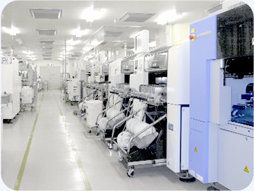
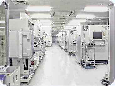
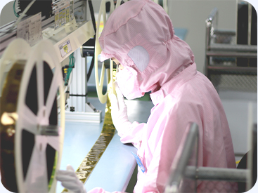
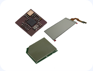
We are capable of performing all processes from wafer test to module mounting in our company.
With the dramatic evolution of electronics, LSI device and module are required to have higher functionality with downsizing. We, in order to meet these market demands, are producing latest LSI device and module by integrating technologies, equipment and systems with installing newest equipment and building efficient production system.
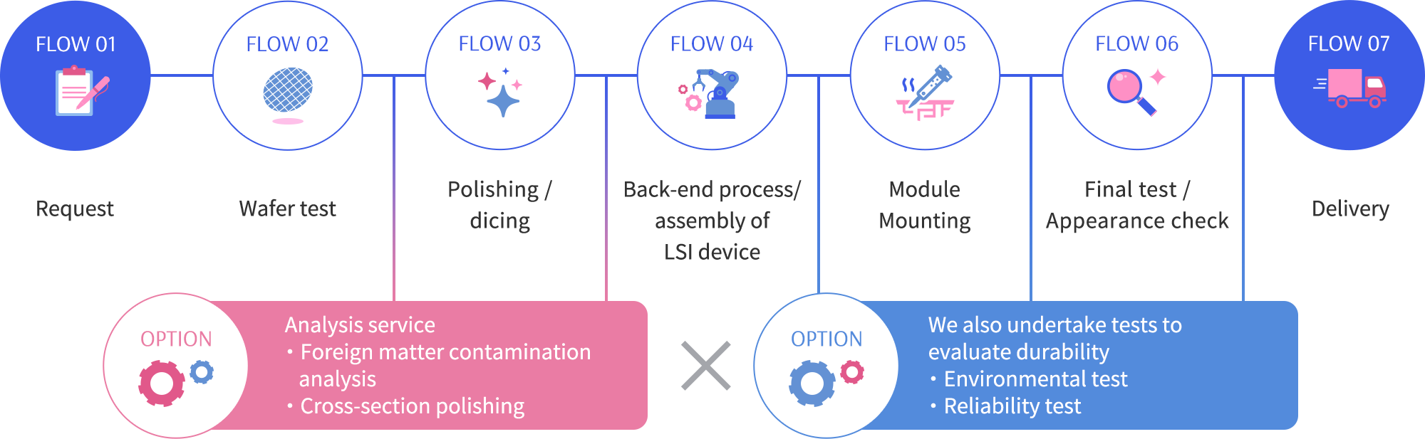
(We can perform sole testing services such as environmental tests and reliability tests.)
FLOW 01
We support manufacturing products according to requirements of a customer.
Please feel free to contact us.
FLOW 02
Wafer test of the product.
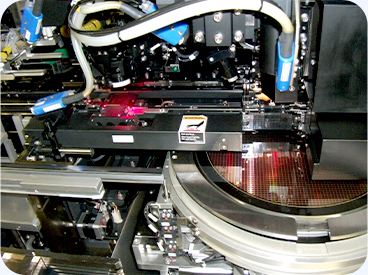
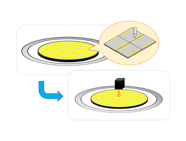
FLOW 03
Backside polishing, laser grooving,
Wafer dicing
FLOW 04
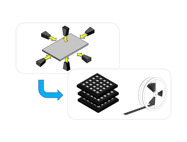
Assembly with our unique technology and technique
Die bonding
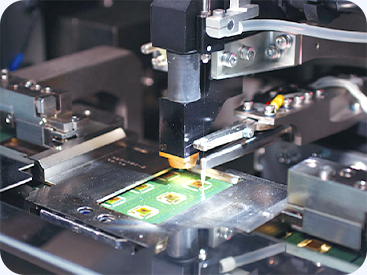
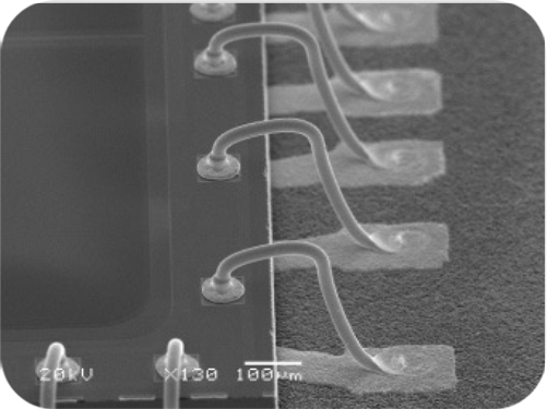
Wire bonding /
Bump bonding
Flip chip bonding
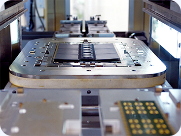
Molding
FLOW 05
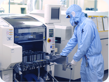
Mounting modules and products with inspection
FLOW 06
Final test before delivery
Check and inspect product performance in details
FLOW 07

We support one-stop service from request to delivery
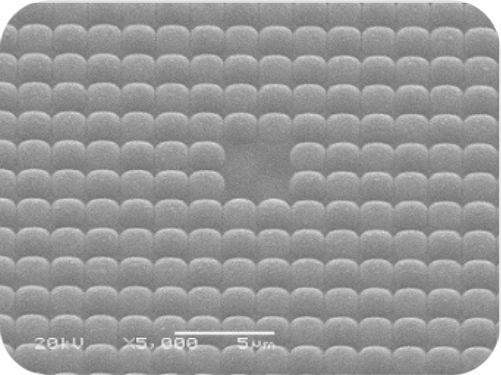
Observe the internal structure of devices in detail and visualize minute internal defects and defective structures.
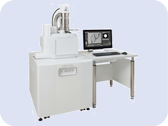
■Example: SEM observation image

Reliability testing service for electronic components
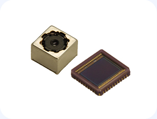
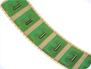
We support automated assembly lines for lens, AF unit, lid glass, sensor cover, image sensor, board, FPC etc. By cleaning the process, we can handle high pixel products with high yield.
We support downsizing with high-density mounting and small packaging technology. We support FPC mounting (ACF, soldering), and support electromagnetic shield technology.
We support mounting of surrounding parts. We support multiple chips (multi-chip).
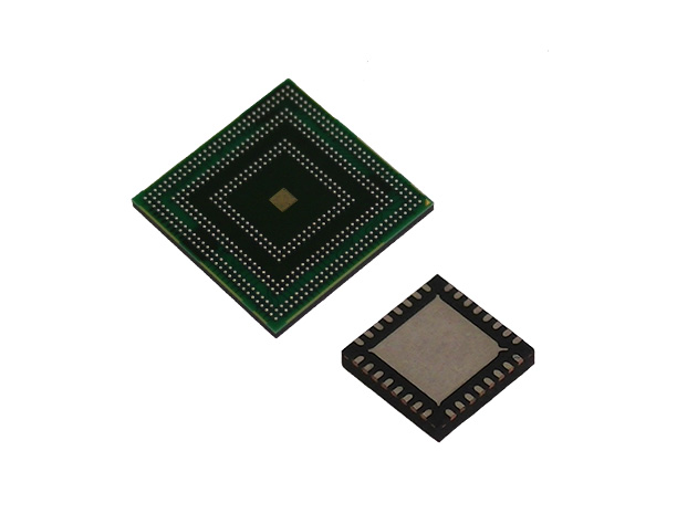
We support multi-functioning by multi-stacking of ICs. The plastic Burrs on terminal surface are removed by special laser, and this ensures stable solder wettability.
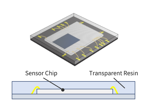
We support a packaging which uses transparent mold resin. This packaging is ideal for light sensing devices. High transparency and weather-resistance can be achieved.
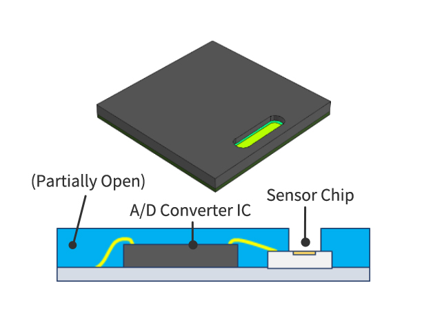
This is a package which exposes the surface of semiconductor by partially opening the mold plastic. The exposing shape can be customized according to the application of electronic part.
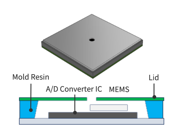
This is a package with cavity is
pre-formed with mold resin and its inside is hollow. The package can be at lower cost compared to the cavity type boards such as ceramic boards.
We can handle 8-inch TAIKO®wafer mounting, rib removal, and dicing. After processing, shipping form can be in rings, chip trays, and embossed reels.
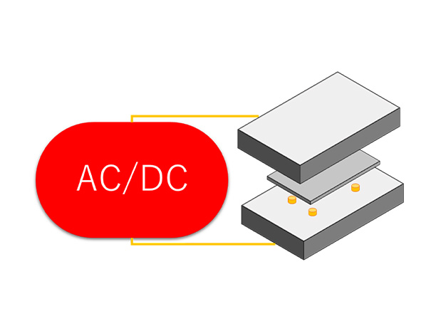
We support AC/DC test for individual chips. We can handle and perform chip test for home appliances and automobiles.
After processing wafers into chips, it is possible to perform high-precision visual inspection of six sides of the chip using an automatic visual inspection machine. After the inspection, the chip can be shipped as KGD in various packaging forms.
We support wire bumping and dicing for max 12 inch wafers. After processing, all products are visually inspected and measured using an automatic inspection machine.
It is possible.
We confirm and discuss the specification of the prototype in advance.
Basically, it is possible.
However, if the customer uses special materials for the product, considering MOQ, the some cost might be account of the customer. Please contact us in advance for details.
It is possible.
We require the data of the trial production and evaluation to be shared. With our evaluation, we identify further issues and the points to be improved which aim for mass production.
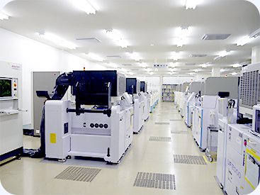
We are confident on our manufacturing line as the line is always built in the optimum environment with ESD management by ESD coordinators who has professional qualifications.
*) This is a system in which RCJ (Reliability Center for Electronic Components of Japan) certifies ESD coordinators based on the IEC61340 series standard.
It is depending on the details of the inquiry, please contact us for the details first.
We have acquired ISO9001 / IATF16949 certification and have sufficient experience of mass production of in-vehicle products.
S-TAKAYA is registered as a medical device manufacturer. Please contact us for each product.
We do not support for the optical design. Please supply as a part.
It is possible.
Both sheet and individual board / substrate are available. Rigid-flex is also available.
It is possible as we have a flux cleaning machine.
The minimum we support is 0402.
It is possible.
We have both an SMT line and a solder ball mounting line. We support from the material selection, please feel free to contact us.
It is possible.
We have equipment that can handle up to 30 pitches (142.5 mm). We can mount it with electrical characteristic check, please feel free to contact us.
It is possible.
We have the appropriate equipment that can handle the requirement. Please feel free to contact us.
It is possible.
We have the appropriate equipment that can handle the requirement. Please feel free to contact us.
It is possible.
We have the appropriate equipment that can handle the requirement. Also, we can perform the reliability test at the same time. Please feel free to contact us.
Basically, we do not support both rework and reball.
We support quick inspections (such as BGA) and internal inspections of the electronic parts packages. However, as we mainly perform partial inspections, please contact us for the project which requires a large amount of inspection.
It is possible.
We have a vacuum degassing sealer.
It is possible.
Please feel free to contact us.
It is possible as we have an equipment which removes Low-k materials. Please feel free to contact us.
It is possible.
We consider the possibility including the conversion to our own tester, please feel free to contact us.
It is possible.
We have experience on the tests for inner void & crack, delamination analysis and wire conditions, etc.
For details, please feel free to download the documents.
Also, if you have detailed requirement, please feel free to contact us.
It is possible.
However, it is limited to the materials prepared by us. In addition, we can support on various legal related documents and RoHS directives. Please contact us first.
